MHC-WLED ESP32-P4 shield — hardware reference¶
Terminal pinout and onboard features for the MHC-WLED ESP32-P4 shield (myhome-control), the P4-NANO carrier used on the bench (catalog deviceModel: "MHC-WLED ESP32-P4 shield", esp32p4rev1-eth firmware). Read from the board silkscreen + the builder's schematics so projectMM work reads this instead of the marketing render. The shield sits on a Waveshare ESP32-P4-NANO; GPIO numbers are the P4's.
Board revision: the terminal map and RS-485 wiring below are transcribed from a V1 board (the builder's labelled V1 photos + schematics). The overview render is a V2 render. Whether V2 keeps the identical GPIO↔terminal wiring is not confirmed here — treat the map as V1-specific and verify against your own board's silkscreen if you have a different revision.
Sources
- Overview render (board V2): docs/assets/deviceModels/mhc-wled-esp32-p4-shield.jpg
- Silkscreen (photographed) + the builder's V1 schematics and terminal maps (myhome-control / Wladi, 2026-07-16); the transcriptions below come from those. The schematics supersede the marketing render where they differ.
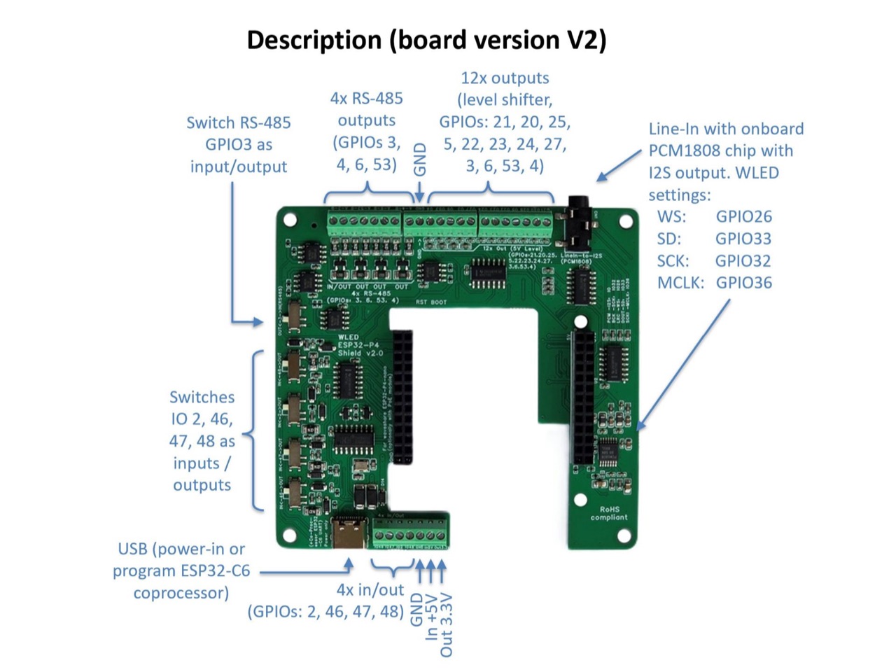
Pinout¶
GPIO ↔ screw-terminal map (V1 board)¶
The output/RS-485 terminals, left to right, with the P4 GPIO each carries:

O21 O20 O25 O5 O7 O23 O8 O27 O3 O22 O24 O4 — the level-shifted single-ended LED outputs, then the four RS-485 differential pairs.
Nothing on this shield is a bare GPIO. Every terminal routes through protection or level-shifting — the reason a direct drive-and-read WS2812 loopback jumper fails on it (see below). Four terminal groups:
12x outputs — level-shifted, single-ended (LED data)¶
The LED-data outputs. Each terminal is O<gpio> on the silkscreen; a level shifter drives the 5 V strand from the P4's 3.3 V. The catalog wires the Parallel LED driver (peripheral Parlio) to the first eight (21,20,25,5,22,23,24,27).
| Terminal | GPIO | Note |
|---|---|---|
| O21 O20 O25 O5 O22 O23 O24 O27 | 21 20 25 5 22 23 24 27 | LED lanes (Parallel LED, peripheral Parlio, default) |
| O7 / O8 | 7 / 8 | also the I²C bus (SDA 7 / SCL 8, catalog I2cScan) |
| O3 | 3 | also on RS-485 (A-3-B) — see note below |
| O4 | 4 | also on RS-485 (A-4-B) — see note below |
| GND | — | ground for the output block |
GPIO 3, 4, 22, 24 each appear TWICE — once here (level-shifted single-ended output,
O<n>) and once in the RS-485 block (A-<n>-B). It's the same P4 GPIO fanned out to two output forms: driving the pin lights up both itsO<n>terminal and itsA-<n>-Btransceiver at once. Wire to whichever form you need. GPIO 21/20/25/5/23/27 have only the level-shifted path (no RS-485), which is why the LED-driver default uses those + 22/24 for strips and leaves 3/4 free.
4x RS-485 — differential A/B pairs (range extender + DMX)¶
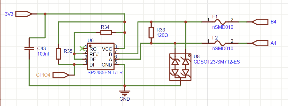
Each channel is A-<gpio>-B on the silkscreen: an RS-485 transceiver (an SP3485EN-L/TR, not a bare GPIO) driven by that GPIO, with 120 Ω termination, resettable fuses (nSMD010), and TVS protection (CDSOT23-SM712-ES) on the line. Each channel occupies TWO screw terminals — an A and a B (the differential pair), so the 4 channels are 8 terminals total. Channels on GPIO 4, 22, 24, 3.
RS-485 is here for two purposes:
- Range extender — RS-485's differential pair carries LED data far past what a single-ended 5 V line manages. At the LED end you need an RS-485 receiver with a 5 V data output to convert the differential signal back to the WS2812 single-ended waveform.
- DMX-512 output — DMX's physical layer is RS-485, so these channels double as DMX outputs. Wire an XLR connector to
GND,<n>A,<n>B; in DMX nomenclature A is Data− (Signal−), B is Data+ (Signal+).
Three channels are transmit-only; one (GPIO 3) is switchable. On the transmit-only channels (GPIO 4, 22, 24) the transceiver's RE#/DE direction pins are hard-wired to transmit (DI in, RO disconnected):
The GPIO 3 channel adds a mechanical slide switch (SW5, MSK12C02) that ties the transceiver's RE#/DE to 3V3 or GND — i.e. it selects transmit mode (DI, GPIO 3 drives the line) or receive mode (RO, GPIO 3 reads the line):
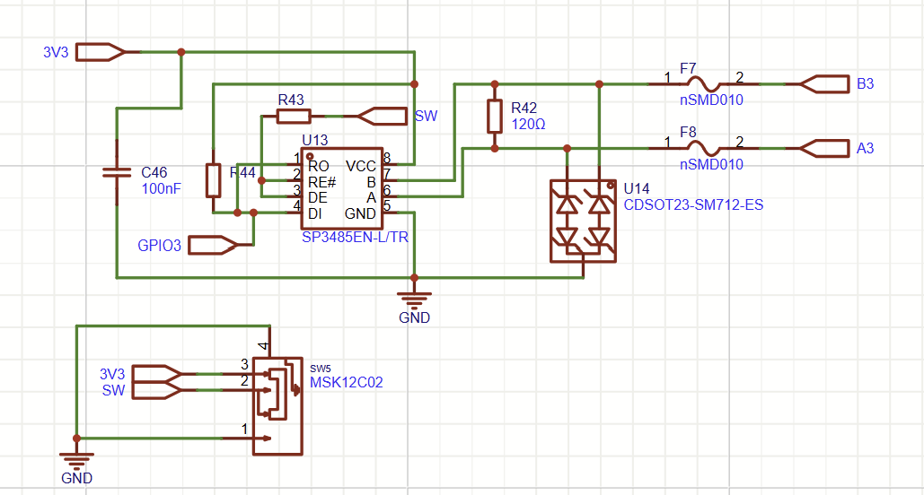
| Channel | GPIO | Terminals | Direction |
|---|---|---|---|
| A-4-B | 4 | A4, B4 | transmit only |
| A-22-B | 22 | A22, B22 | transmit only |
| A-24-B | 24 | A24, B24 | transmit only |
| A-3-B | 3 | A3, B3 | transmit or receive (board switch) |
4x in/out header¶
The O46 O47 O2 O48 header plus power (GND, In5V, Out3V3):
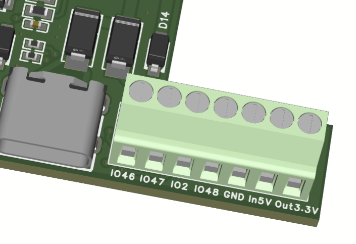
Inputs are diode-protected with a ~16 kHz low-pass filter — designed for robust button-style inputs, not high-speed signals. GPIO 2 and 46 are P4 boot straps. This header is not usable for a WS2812 loopback (the filter and protection destroy the ~800 kHz waveform).
Line-In audio (PCM1808 → I²S)¶
An onboard PCM1808 ADC captures a line-in signal and outputs I²S to the P4. Catalog AudioService: SCK 32 · WS 26 · SD 33 · MCLK 36 (the P4 is I²S master, so it drives MCLK).
Ethernet (RMII)¶
The P4-NANO's RMII PHY: MDC 31 · MDIO 52 · RST 51 · CLK 50 (external-in) · PHY addr 1, ethType IP101, external clock. (Catalog NetworkModule.)
Loopback self-test on this shield¶
The loopback self-test drives a WS2812 frame out one pin and reads it back on a jumpered pin — so it needs a signal path from a Tx pin to an Rx pin. The bare-GPIO terminals can't provide it (every one is buffered), but the GPIO 3 switchable RS-485 channel can, because its board switch turns GPIO 3 into a data input:
- Set the GPIO 3 board switch to the receive (input) position, then jumper the RS-485 differential pairs
A4→A3andB4→B3(the wiring the builder shows):
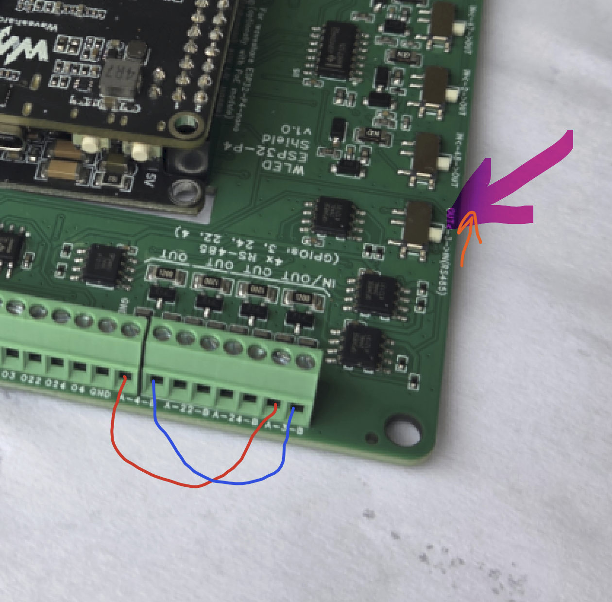
- The signal path is: GPIO 4 emits the WS2812 frame → the first RS-485 transceiver drives it as a differential signal on
A4/B4→ the second transceiver reads it back → GPIO 3 receives it as a 3.3 V data input. So the loopback runs Tx = GPIO 4, Rx = GPIO 3 with the switch in the input position. - The bare P4-NANO already proves the frame-size fix directly (GPIO 32↔33, PASS at every grid size), so the shield doesn't need to re-prove it — but this RS-485 path is the builder's intended on-shield loopback, distinct from the bare-GPIO jumper the self-test defaults to.
- To verify LED output on the shield, the other honest test is to wire a real WS2812 strip to an
O<n>output and watch it light — that exercises the true path (GPIO → level shifter → strip), which is what the shield is built for.
Cross-reference¶
Chip-level GPIO constraints (straps, flash/PSRAM) for the P4 are in gpio-usage.md § ESP32-P4; this page is the board wiring. The catalog entry is mooninstaller/deviceModels.json (MHC-WLED ESP32-P4 shield). RS-485 / DMX-512 as a first-class projectMM output is tracked in the RS-485 / DMX-512 wired-output backlog item.